
Modeling, Prediction, and Results Correction of PDSH Circuits for Nanosecond Pulse Peak Detection

School of Information Science and Technology, Fudan University, Shanghai 200433, China
*
Author to whom correspondence should be addressed.
Appl. Sci. 2023, 13(23), 12597; https://doi.org/10.3390/app132312597
Submission received: 23 October 2023
/
Revised: 20 November 2023
/
Accepted: 21 November 2023
/
Published: 22 November 2023
(This article belongs to the Special Issue Advanced Electronics and Digital Signal Processing)
Abstract
:The peak detect and sample hold (PDSH) circuit is an important component of the light detection and ranging (LiDAR) system, because the PDSH circuit can correct the walk error of the time discriminator, and distinguish different objects at the same location. However, due to the requirement for high-precision measurement of nanosecond-scale pulse signals, the design of the PDSH circuit presents significant challenges. This paper accomplishes the modeling of the PDSH circuit, including the modeling of the PDSH measurement speed and the voltage step, quantifies various factors that affect the PDSH circuit measurement results, and makes predictions based on the model. Through the derivation and simplification of the rise process in the PDSH circuit, this study establishes a mathematical model to predict the performance of the PDSH circuit. Furthermore, this study also investigates the effect of circuit delay time on the measurement speed of the PDSH circuit. Meanwhile, this study analyzes the voltage step process, and an equivalent circuit model is derived through theoretical analysis. By utilizing a fitting method, the equivalent capacitance value of the diode is obtained. The simulation and experiment results show that the errors between the measurement speed model of the PDSH circuit and the actual circuit are no more than 1.98 ns and 2.03 ns, respectively. Thus, the measurement speed model can accurately predict whether the PDSH circuit meets the requirements. Moreover, the maximum absolute error of the equivalent circuit model is 19.87 mV, which can significantly reduce the error caused by the voltage step.
1. Introduction
The peak detection and sample hold (PDSH) circuit is important in the pulsed time of flight (ToF) light detection and ranging (LiDAR) system [1,2,3,4,5]. The PDSH circuit captures the pulse signal and obtains the accurate amplitude of the signal, which provides precise distance information for the ToF LiDAR system. However, with the development of ToF LiDAR systems, the pulse width that needs to be detected reduces, while the accuracy requirement intensifies significantly [6]. Especially when the pulse width approaches the nanosecond domain, the LiDAR system requires a very fast response [7]. Furthermore, in the nanosecond domain, the parasitic parameters, such as parasitic capacitance and parasitic resistance, deteriorate the magnitude response, and accordingly affect the distance information required by the ToF or LiDAR system [8,9]. Therefore, designing PDSH circuits for nanosecond pulse peak detection is both important and challenging [10,11,12,13,14].
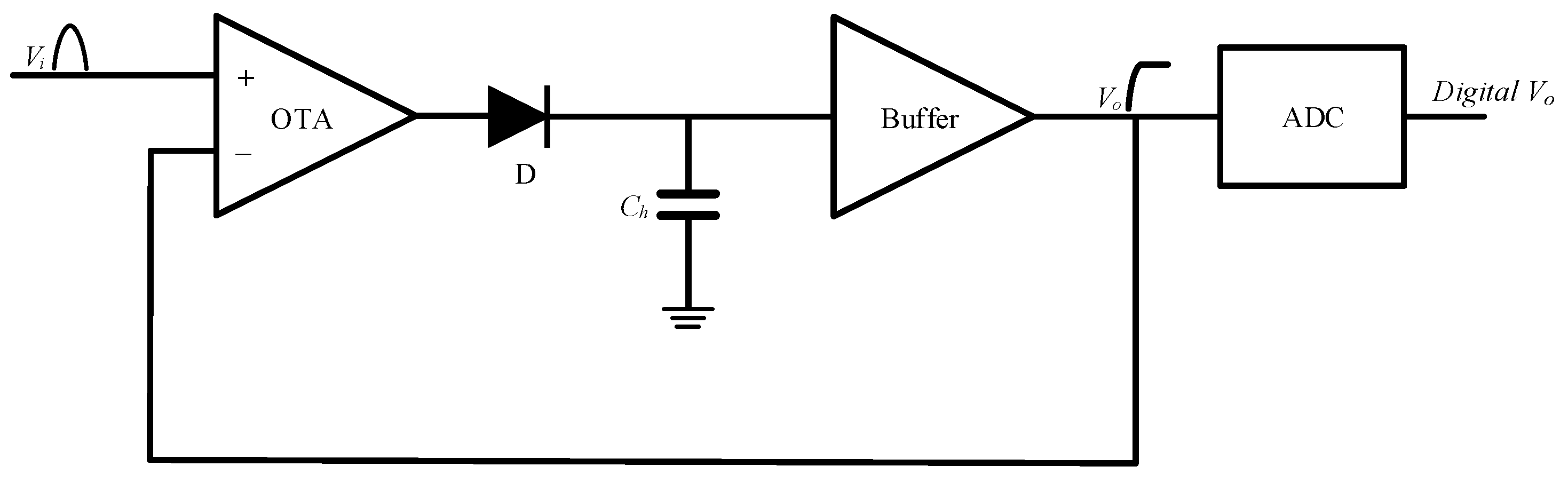
The most widely used CMOS-based PDSH circuit in industry is shown in Figure 1 [15]. The circuit charges a capacitor through a switch, either a diode or a MOS. When the input voltage Vi is greater than the output voltage Vo on the sampling capacitor Ch, the switch is turned on, and the input voltage charges the capacitor. Conversely, the switch is turned off, and capacitor Ch maintains the peak voltage, which can be measured using the ADC sampling method [16,17,18]. Therefore, the control signal of the switch will directly affect the measurement of the pulse peak. However, the circuit is only valid for ms-scale pulse width detection and needs to be improved for ns-scale pulse width detection.
Dlugosz et al. [19] proposed a PDSH circuit using a current-mode latching mechanism and flag generation circuitry to control the switch, which had shallow energy consumption. However, it can only measure the ms-scale pulse width. Jayaraman et al. [20] also designed a CMOS peak detector, which used CMOS to control the charging and discharging of the capacitor. However, the driving ability is relatively small, and the measurement accuracy decreases.
The OTA-based PDSH circuit with negative feedback can overcome the shortcomings of the PDSH circuit [21,22,23]. Haas et al. [21] proposed an improved PDSH circuit, which would take the output voltage as input to the negative input of the transconductance operational amplifier (OTA) and use the voltage Buffer to output the result. Hao et al. [22] used OPA615 to build the PDSH circuit, analyzed the circuit’s bandwidth, and completed the measurement of the pulse peak of 100 ns pulse width and 20 kHz repetition frequency. Moreover, Zhang et al. [23] used the same circuit to measure the peak value of a laser pulse with a pulse width of 200 ns. The PDSH circuit based on OTA IC chips has the advantages of easy construction, fast measurement, low cost, and convenient use. As the output current of OTA is variable, the circuit overshoot is slight. The OTA’s maximum output current limits the circuit’s maximum measurement speed, and the voltage step phenomenon will lead to significant measurement errors.
To overcome the error caused by the voltage step of the PDSH circuit based on OTA, a CMOS PDSH circuit was proposed by Kruiskamp [24], where a current mirror was used instead of a diode to nonlinear solute problems caused by the diode. However, it also produces new problems, such as significant overshoot, large pedestal voltage, and tradeoffs between measurement accuracy and speed. Geronimo et al. [25] proposed the two-phase peak detector to overcome the tradeoff between measurement accuracy and speed. Nevertheless, it can only measure the μs-scale pulse width. Recently, Zheng et al. [2] presented an auto-adjust charging current CMOS PDSH circuit, which reduced errors caused by the pedestal voltage and overshoot voltage. Similarly, Ma et al. [3] proposed using a controlled current source instead of a current mirror to reduce the error. However, there is still the problem of slow measurement. Thus, CMOS PDSH circuits improve some problems of PDSH circuits based on OTA chips but also have disadvantages, including inconvenient construction and higher cost, in addition to the above.
In summary, CMOS PDSH circuits have drawbacks such as slow measurement speed, large pedestal voltage, and overshoot voltage, as well as a long production cycle. Although the OTA-based PDSH circuit can decrease the pedestal voltage and the overshoot, the voltage step phenomenon results in significant measurement error. Therefore, neither the CMOS-based PDSH nor the OTA-based PDSH circuit can meet ns-scale pulse peak detection. In order to accurately measure the peak value of nanosecond pulse signals, this study undertook a comprehensive theoretical modeling of the PDSH circuit. The accurate modeling aims to identify the primary factors that influence the measurement speed of the PDSH circuit. Meanwhile, in order to correct the voltage step error in PDSH circuit measurements and improve measurement accuracy, this study also proposes an equivalent circuit modeling approach for the voltage step process in the PDSH circuit. This equivalent circuit predicts the error due to the parasitic parameters. Finally, the study corrects the predicted error. With these three steps, i.e., modeling, prediction, and results correction, the proposed method can meet both the time requirements and voltage step requirements of ns-scale pulse peak detection.
The rest of this paper is organized as follows. Section 2 investigates the PDSH circuit based on OTA, and the mathematical model is built to describe the main factors affecting PDSH measurement speed. Meanwhile, Section 2 also presents the equivalent circuit model. The simulations and experiments are carried out to verify the mathematical and equivalent circuit models’ correctness in Section 3. Finally, Section 4 concludes this paper.
2. Modeling of the PDSH Circuit
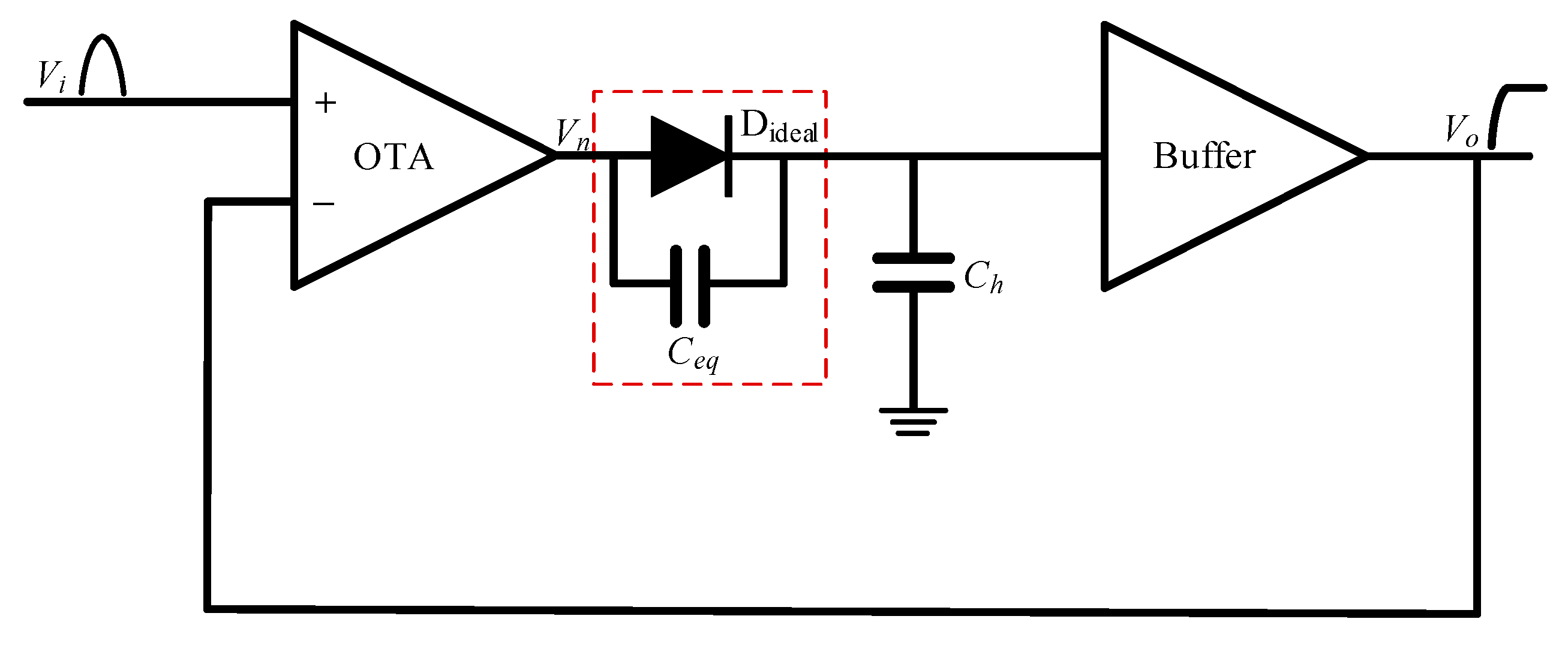
The PDSH circuit based on the OTA chip consists of OTA, diode, sampling capacitor, and voltage Buffer, as shown in Figure 2. OTA can amplify and convert the difference between the non-negative input voltage Vi and the negative input voltage Vo into the output current Io. Therefore, if the input voltage Vi is greater than the output voltage Vo, the output current of OTA charges the sampling capacitor Ch through diode. While Vi is smaller than Vo, the diode is reverse-biased, and the PDSH circuit is forced into a hold state. Subsequently, the output voltage of the PDSH circuit is determined as the peak value of pulse signal, and it can be acquired by using a low-speed ADC.
The voltage–current characteristic curve of OTA is commonly classified into two main regions, namely the linear region and the saturation region. When the differential input voltage is less than the threshold voltage Vth, the OTA operates in the linear region, and the output current Io can be described by (1), where g is the transconductance of OTA.
When the differential input voltage is greater than the threshold voltage Vth, the OTA operates in the saturation region, and the output current remains at the maximum output current Iom, expressed as (2).
The actual OTA devices exhibit a linear offset in the output current in the saturation region, denoted by k. Therefore, the output current Io in the saturation region can be described (3) and (4).
2.1. The Measurement Speed of the PDSH Circuit
The measurement speed of the PDSH circuit is a critical factor determining whether the PDSH circuit can accurately measure the peak value of a pulse. Therefore, an analysis of the measurement speed of the PDSH circuit is conducted here.
The input pulse signal Vi is assumed to consist of three stages: rising period, plateau period, and falling period, as shown in Figure 3. In the rising period, the input voltage Vi can be described by (5), where tr represents the rise time. And in the falling period, Vi can be described by (6), where tf is the fall time. During the plateau period, Vi maintains a constant peak value Vm, and the duration is th.
When the assumed pulse signal Vi is applied as the input to the PDSH circuit, the output voltage of the PDSH circuit without considering delay is shown in Figure 3.
Initially, the OTA operates in the linear region, and the output voltage Vo can be expressed by (7).
Using the difference between the input voltage Vi and the output voltage Vo as the variable, (7) can be rewritten as (8).
According to the initial conditions ΔV(0) = 0, the solution of the equation is expressed as
The difference between the input voltage and the output voltage is equal to ChVm/gtr. The condition for the OTA to not enter saturation region can be expressed as (10). According to (2), the condition can also be expressed as (11)
The difference between the input voltage and output voltage is no more than Vth at this time. Since Vth is very small, the measurement speed of the PDSH circuit meets the requirements for detecting the peak value of the pulse signal when (11) is satisfied.
However, when the OTA enters the saturation region, the difference between the input voltage and the output voltage gradually increases, indicating that the measurement speed of the PDSH circuit is insufficient, and the output voltage cannot keep up with the input changes.
Assuming that the PDSH circuit enters the saturation region at time t0 and returns to the linear region at time t1, the output voltage of the PDSH circuit during the time interval from t0 to t1 can be expressed by (12).
The solution of (12) can be obtained by incorporating the output voltage at time t0, but it is not intuitive to observe the main factors that affect the PDSH output voltage. Therefore, a simplification of (12) is necessary. As the value of k is very small, Equation (12) can be simplified to
Furthermore, due to the short time that OTA works in the linear region and the relatively small output current, it can be assumed that the output voltage of the PDSH circuit is described by (12) during the entire charging phase of the sampling capacitor. At this point, the output voltage Vo can be expressed as
Therefore, the measurement speed of the PDSH circuit can be described as
The main factors affecting the measurement speed of the PDSH circuit are the maximum output current of the OTA Iom and the sampling capacitance Ch, as indicated by (11) and (15).
The error mainly stems from two simplification processes during the charging of the sampling capacitor. During the simplification process, the influences of the parameters Vth and k are mainly neglected, as well as the charging current when the OTA is operating in the linear region. The delay of both devices and circuits is also one of the sources of error in the simplified model.
In conclusion, the measurement speed of PDSH circuit is sufficiently fast to enable the output voltage to fully keep up with the input signal, when (11) is satisfied. However, when (11) is not satisfied, the measurement speed can be expressed by (15), and in this case, the PDSH circuit needs to spend some time to measure the peak value of the pulse signal.
2.2. The Calibration of Voltage Step Error
Measurement accuracy is another important requirement of the PDSH circuit. The OTA-based PDSH circuit exhibits a low pedestal voltage and a small overshoot voltage due to the adjustable output current of the OTA with respect to the input voltage. However, due to the presence of diodes, the OTA-based PDSH circuit has relatively large measurement errors caused by the voltage step phenomenon.
When the PDSH circuit completes the peak value measurement of the pulse, the output voltage of the OTA is equal to the negative saturation voltage of the OTA [10,24]. At this moment, the diode switches from forward bias to reverse bias. When a diode is forward-biased, current flows through the diode, causing the diffusion of electrons and holes and giving rise to the existence of the diffusion capacitance. In the case of reverse bias, the diode is in a cutoff state, but due to the presence of a certain amount of charge carriers in the depletion region, the depletion capacitance exists at this time. During the transition of a diode from forward bias to reverse bias, both the diffusion capacitance and depletion capacitance must absorb charge from the sampling capacitor. As a result, the sampling capacitor will discharge when the diode changes from forward bias to reverse bias, resulting in the step voltage error as shown in Figure 3. Due to the nonlinearity in the variation of depletion capacitance with reverse bias voltage, the analysis of voltage step processes becomes highly intricate. To simplify the analysis, an equivalent capacitor was used to realize the equivalent process of the diode from forward bias to reverse bias. Therefore, during the transition of the diode from forward bias to reverse bias, an ideal diode and an equivalent capacitor Ceq were used in parallel for equivalent substitution, as shown in Figure 4.
In order to correct the voltage step error, it is necessary to establish the relationship between the final output voltage Vf and the peak voltage Vm.
When the PDSH circuit completes the peak value measurement of a pulse signal, the voltage on the sampling capacitor is equal to the peak voltage Vm, and the output voltage of the OTA is higher than the peak voltage Vm by the forward voltage of a conduction diode Von. Subsequently, the output voltage of OTA rapidly changes to the negative saturation voltage of OTA Vn, and the sampling capacitor charges the equivalent capacitor until reaching the final voltage Vf.
According to the law of conservation of charge, the following equation holds.
The final voltage Vf can be expressed as
The value of the voltage step can be described as
Therefore, the important factors affecting the voltage step error include the equivalent capacitance of the diode, the sampling capacitance, the peak value of the pulse voltage, the forward voltage of the diode, and the negative saturation voltage of the OTA. The paper measures the final voltage Vf at different sampling capacitance Ch and fits the data by using (18) to determine the equivalent capacitance of the diode.
Furthermore, the magnitude of the voltage step can be calculated using (18), which can be used to correct the measurement results of the PDSH circuit and reduce the voltage step error.
3. Circuit Simulation and Experiment
Simulation and experimental circuits for the PDSH circuit are constructed, according to Figure 2. Considering the measurement of nanosecond-scale pulse peak, OTA should possess features of high bandwidth, high slew rate, and low delay. In this paper, the OPA615 chip is selected as the OTA to construct the PDSH circuit. The parameters g, Vth, Iom, and k can be obtained by DC scanning of the OPA615 by using the simulation software. Following that, the diode uses the simulation model of 1N4148. The simulation circuit diagram of the PDSH circuit in PSpice is shown in Figure 5.
The schematic diagram and experiment diagram of the overall system are shown in Figure 6 and Figure 7, respectively. The pulse signal is generated by the signal generator RIGOL DG4602, while employing FPGA triggering techniques to achieve pulse widths in the nanosecond range. And the power supply for the experimental PCB board is provided by the DC power supply RIGOL DP831, while the signal measurements are performed using the oscilloscope Agilent DSO7104B. After the completion of the PDSH circuit measurement, in order to measure the peak value of a single pulse signal, the FPGA was utilized to control the discharge of the sampling capacitor through the MOSFET. This discharge was performed to prevent any interference from the previous measurement, ensuring the accuracy and reliability of the current measurement. Furthermore, OrCAD Capture 16.6 (PSpice) software was also used to verify the results of the model.
Figure 8 illustrates the dynamic measurement process of the PDSH circuit with Ch = 30 pF, tr = 10 ns, and Vm = 1 V. Since the maximum output current of OPA615 is 5 mA, which satisfies (11), the output voltage of the PDSH circuit can keep up with the input signal variation. The horizontal axis represents time, while the vertical axis represents voltage. The simulation results indicate that the difference between the input and output voltages is always smaller than the threshold voltage, shown as (b), which is consistent with the theoretical prediction.
Figure 9 illustrates the dynamic measurement process of the PDSH circuit with Ch = 30 pF, tr = 10 ns, and Vm = 3 V. The horizontal axis represents time, while the vertical axis represents voltage. Based on the fact that the charging rate Iom/Ch of the sampling capacitor is smaller than the rising rate Vm/tr of the input signal, the difference between the input and output voltages will be greater than the threshold voltage. Therefore, the PDSH circuit needs to spend a certain amount of time to accurately measure the peak value of the pulse, according to the theory.
Figure 8 and Figure 9 also show that the slew rate of the OTA is lower than the rise rate of the input signal. Although the OTA will charge the capacitor at the maximum output current at this time, the output voltage of the PDSH circuit still cannot keep up with the input signal.
The measurement speed of the PDSH circuit can also be characterized by the rising time of the output voltage. The derivative of the output voltage with respect to time reflects the instantaneous measurement speed of the PDSH circuit, while the rising time can reflect the average measurement speed.
In this paper, the Simulink tool in MATLAB was used to model the measurement process of the PDSH circuit. Simulink allows the insertion of delay modules, which enables a more precise description of the measurement process of the PDSH circuit.
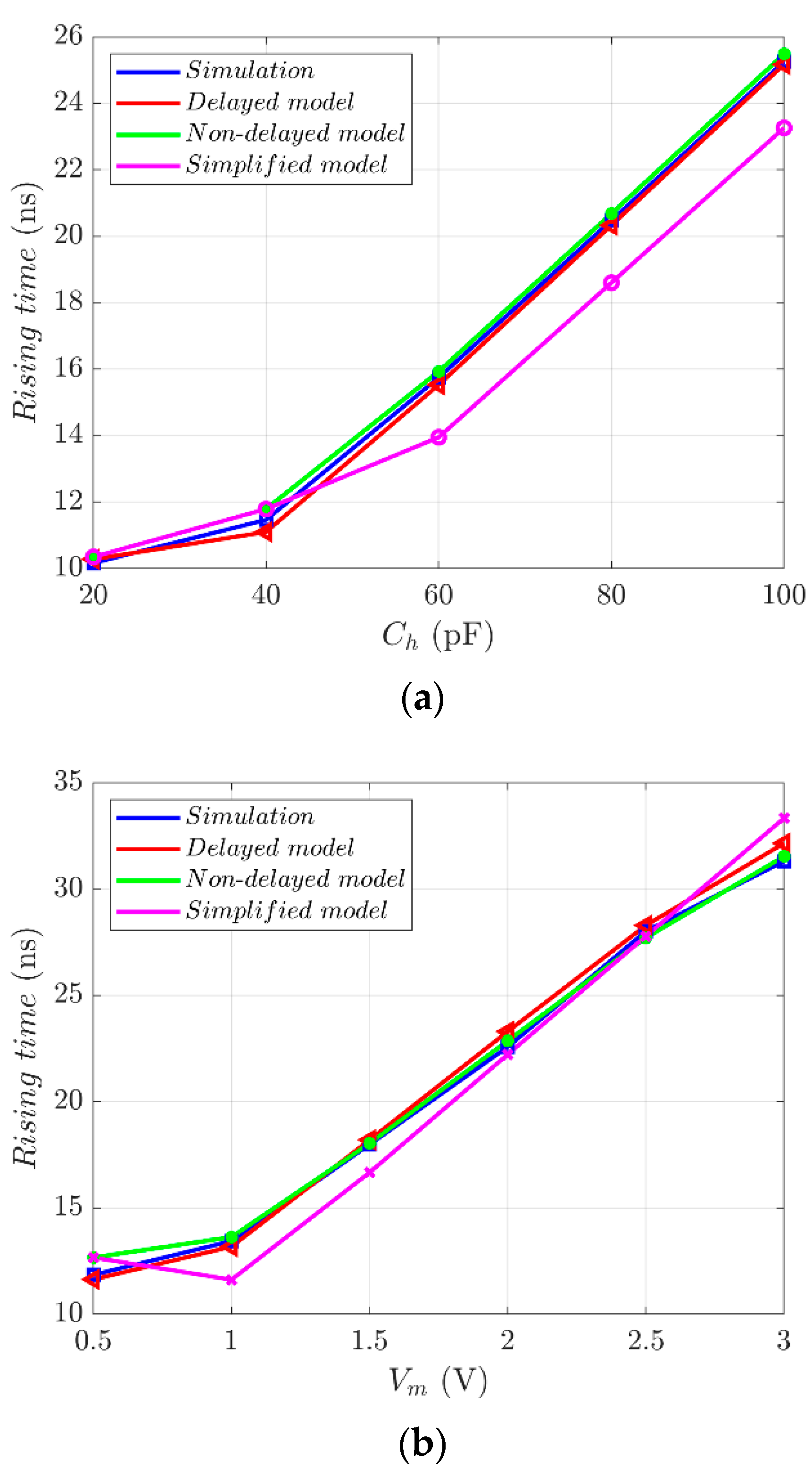
Figure 10a shows the rising time of the output voltage in simulation, delayed model, non-delayed model, and simplified model with different sampling capacitances. And Figure 10b demonstrates the rising time of the output voltage under different peak values of the input signal. The figure indicates that the delay time, as a secondary factor, can also have an impact on the measurement speed of the PDSH circuit. Meanwhile, the maximum error between the simplified model and the simulation results is 1.98 ns when Ch is 100 pF, indicating that the simplified model can accurately describe the measurement speed of the PDSH circuit.
Figure 10 shows that the main source of error in the simplified model is not the delay time of the system but the simplification of the capacitor charging process, and the error is within the acceptable range.
Figure 11 illustrates the rising time of the output voltage for experimental, delayed model, and simplified model at different peak voltages. The results indicate that the maximum error between the simplified model and experiment results is 2.03 ns.
Simulations and experiments show that the simplified model can accurately and simply describe the measurement speed of the PDSH circuit.
In order to quantitatively describe the step voltage error, the equivalent capacitance Ceq of the diode must be solved. According to (18), the equivalent capacitance Ceq can be obtained by fitting the data based on the final voltage Vf under different sampling capacitance Ch. The change of equivalent capacitance of the diode can be achieved by changing the junction capacitance of the diode in the simulation software.
Figure 12 illustrates the relationship between the final output voltage Vf and the sampling capacitance Ch for different diode junction capacitances Cj when the peak voltage Vm is 2 V. The horizontal axis represents the sampling capacitance Cj, while the vertical axis represents the final voltage Vf. The simulation results are represented by dots, and the fitting curve based on (18) is shown as a solid line. Therefore, the equivalent capacitance Ceq of the diode can be calculated according to (18). Figure 12 shows that the relationship between the final output voltage and the sampling capacitance follows (18), which verifies the correctness of the voltage step model.
Based on the above method, several types of diodes are experimentally measured for their equivalent capacitance Ceq, and the results are shown in Table 1. The reverse recovery time Trr and diode capacitance Cd are obtained from the datasheet.
The simulation results in Figure 13 show that the final output voltage Vf varies linearly with the peak voltage Vm at different equivalent capacitance Ceq. The solid line represents the fitting curve obtained from (18), and the dots represent the simulation results. The horizontal axis represents the peak value of input pulse signal, while the vertical axis represents final voltage. Due to the existence of voltage step, there is a threshold for the measurement of the PDSH circuit, and the output of the PDSH circuit is 0 V when the peak voltage is less than the threshold. According to (18), the magnitude of the threshold is determined by the relative values of the equivalent capacitance Ceq and the sampling capacitance Ch. The linear relationship between the final output voltage Vf and the peak voltage Vm is also confirmed in experiments using different types of diodes, as shown in Figure 14.
Figure 13 and Figure 14 verify that the final output voltage Vf and peak voltage Vm meet the (18) in both simulation and experiment, thus confirming the accuracy of the voltage step model.
The voltage step error of the PDSH circuit can be corrected using the linear relationship between the final output voltage Vf and the peak voltage Vm. Figure 15 illustrates the error between the correction value of the final output voltage Vf and the peak voltage Vm.
The horizontal axis represents the peak value of input pulse signal, while the vertical axis represents the error between peak value and correction value. Experimental results demonstrate that the maximum measurement error of the PDSH circuit after voltage step error correction is 19.87 mV. Therefore, Figure 15 shows that the calibration of voltage step error significantly improves the measurement accuracy of the PDSH circuit.
The preceding section presents a derivation of the factors influencing the measurement speed of the PDSH circuit for nanosecond pulse. Additionally, the equivalent circuit model is established for the voltage step process in the PDSH circuit, effectively reducing voltage step errors. In this section, the simplified model derived in this paper for the measurement speed of the PDSH circuit yields a maximum error of 1.98 ns in simulation results and 2.03 ns in experimental results. In comparison to Haas’ analysis of the dynamic performance of the PDSH circuit [21], as well as the circuit bandwidth analysis conducted by Hao [22] and Zhang [23], the simplified model proposed in this study provides a clear and straightforward approach to determine the capability of the PDSH circuit in accurately measuring nanosecond pulse peak values. Furthermore, in order to mitigate voltage step errors, Kruiskamp [24] and Lipika [10] analyzed the underlying causes of voltage step phenomena and proposed a CMOS PDSH circuit. While the CMOS PDSH circuit successfully avoids the generation of voltage step errors, some new issues are introduced, such as overshoot and pedestal voltage errors. In contrast, this study addresses voltage step errors by establishing an equivalent circuit model for the voltage step process in the PDSH circuit. Experimental results demonstrate that after voltage step error correction, the maximum measurement error of the PDSH circuit is reduced to 19.87 mV. The simplified model solely focuses on the primary factors, which influence the measurement speed of the PDSH circuit and necessitate the integration of circuit dynamic performance and bandwidth for accurate pulse peak value measurements. The holistic approach enables the construction of a rational PDSH circuit that incorporates critical considerations. To further reduce voltage step errors, it is advisable to select diodes with smaller equivalent capacitance, or to utilize a specific circuit configuration to ensure that the output voltage of the OTA exceeds its negative saturation voltage.
4. Conclusions
The measurement speed and accuracy are important characteristics of the PDSH circuit. Therefore, this paper investigates the measurement speed and accuracy of PDSH circuits using OTA-based PDSH circuits. This paper establishes a model for the measurement process of PDSH circuits while also examining the factors that impact measurement speed. Meanwhile, in order to correct errors caused by the voltage step, this paper also proposes an equivalent circuit model for the diode and derives the factors that affect the magnitude of the voltage step error during the hold phase in PDSH circuit.
The simplified model proposed in this study for the measurement speed of the PDSH circuit facilitates accurate predictions of the rise time of the PDSH circuit’s output voltage. The application of the simplified model to forecast the rising time of the output voltage yields a maximum deviation of 1.98 ns and 2.03 ns, respectively, when compared to the results obtained from simulations and experiments. Moreover, after the calibration of the voltage step error, the maximum measurement error of PDSH circuit is 19.8 mV, significantly improving the measurement accuracy of the PDSH circuit. Thus, the modeling and prediction of the PDSH circuit in this study enable the precise measurement of peak values for nanosecond-width pulses to become achievable. However, there are also limitations regarding the application of the model [26,27,28]. Specifically, the voltage step model proposed in this study can only be used to correct the output of the PDSH circuit when the input pulse signal exceeds the threshold voltage. Due to the voltage step, when the amplitude of the input pulse is below the threshold voltage, the output of the PDSH circuit is 0, making using the PDSH circuit a significant challenge to measure and calibrate the extremely weak pulse voltage amplitudes. Therefore, accurately measuring tiny pulse voltage amplitudes is a crucial research focus for the future.
Author Contributions
Methodology, J.S.; Validation, Y.D.; Formal analysis, J.S.; Data curation, Y.D.; Writing—original draft, J.S.; Writing—review & editing, J.S.; Supervision, H.Z., K.L. and J.Q. All authors have read and agreed to the published version of the manuscript.
Funding
This research was funded by Fudan University and Changchun Institute of Optics Joint Foundation, grant number FC2017-002.
Institutional Review Board Statement
Not applicable.
Informed Consent Statement
Not applicable.
Data Availability Statement
The data presented in this study are available in https://github.com/Mrjshu/PDSH-circuit.
Conflicts of Interest
The authors declare no conflict of interest.
References
- Incoronato, A.; Cusini, I.; Pasquinelli, K.; Zappa, F. Single-shot pulsed-LiDAR SPAD sensor with on-chip peak detection for background rejection. IEEE J. Sel. Top. Quantum Electron. 2022, 28, 1–10. [Google Scholar] [CrossRef]
- Zheng, H.; Ma, R.; Wang, X.; Liu, M.; Zhu, Z. A CMOS peak detect and hold circuit with auto-adjust charging current for NS-scale pulse ToF lidar application. IEEE Trans. Circuits Syst. I Regul. Pap. 2020, 67, 4409–4419. [Google Scholar] [CrossRef]
- Ma, R.; Liu, M.; Zheng, H.; Zhu, Z. A 66-dB Linear Dynamic Range, 100-dB· Ω Transimpedance Gain TIA With High-Speed PDSH for LiDAR. IEEE Trans. Instrum. Meas. 2019, 69, 1020–1028. [Google Scholar] [CrossRef]
- Kameyama, S.; Hirai, A.; Imaki, M.; Kotake, N.; Tsuji, H.; Nishino, Y.; Ito, Y.; Takabayashi, M.; Tamagawa, Y.; Nakaji, M.; et al. Demonstration on range imaging of 256 × 256 pixels and 30 frames per second using short wavelength infrared pulsed time-of-flight laser sensor with linear array receiver. Opt. Eng. 2017, 56, 031214. [Google Scholar] [CrossRef]
- Palojarvi, P.; Ruotsalainen, T.; Kostamovaara, J. A 250-MHz BiCMOS receiver channel with leading edge timing discriminator for a pulsed time-of-flight laser rangefinder. IEEE J. Solid-State Circuits 2005, 40, 1341–1349. [Google Scholar] [CrossRef]
- Zheng, H.; Ma, R.; Liu, M.; Zhu, Z. A linear-array receiver analog front-end circuit for rotating scanner LiDAR application. IEEE Sens. J. 2019, 19, 5053–5061. [Google Scholar] [CrossRef]
- Wang, X.; Ma, R.; Li, D.; Zheng, H.; Liu, M.; Zhu, Z. A low walk error analog front-end circuit with intensity compensation for direct ToF LiDAR. IEEE Trans. Circuits Syst. I Regul. Pap. 2020, 67, 4309–4321. [Google Scholar] [CrossRef]
- Ruotsalainen, T.; Palojarvi, P.; Kostamovaara, J. A wide dynamic range receiver channel for a pulsed time-of-flight laser radar. IEEE J. Solid-State Circuits 2001, 36, 1228–1238. [Google Scholar] [CrossRef]
- Ngo, T.; Kim, C.; Kwon, Y.J.; Ko, J.S.; Kim, D.; Park, H. Wideband receiver for a three-dimensional ranging LADAR system. IEEE Trans. Circuits Syst. I Regul. Pap. 2012, 60, 448–456. [Google Scholar] [CrossRef]
- Lipika, P.; Bharath, M.; Suganya, S. Design of High Precision Peak Detect Sample & Hold Architecture for Spectroscopy Applications. In Proceedings of the 2021 International Conference on Emerging Smart Computing and Informatics (ESCI), Pune, India, 5–7 March 2021. [Google Scholar]
- Mandal, S.; Dasgupta, S. Modified CMOS peak detector and sample hold circuit for biomedical applications. In Proceedings of the 2018 Conference on Emerging Devices and Smart Systems (ICEDSS), Tiruchengode, India, 2–3 March 2018. [Google Scholar]
- Achtenberg, K.; Mikołajczyk, J.; Szabra, D.; Prokopiuk, A.; Bielecki, Z. Optical pulse monitoring unit for Free Space Optics. Opto-Electron. Rev. 2019, 27, 291–297. [Google Scholar] [CrossRef]
- Chow, H.; Hor, Z. A high performance peak detector sample and hold circuit for detecting power supply noise. In Proceedings of the APCCAS 2008-2008 IEEE Asia Pacific Conference on Circuits and Systems, Macao, China, 30 November–3 December 2008. [Google Scholar]
- Achtenberg, K.; Mikołajczyk, J.; Szabra, D.; Prokopiuk, A.; Bielecki, Z. Peak detection unit for Free-Space-Optics receiver. Metrol. Meas. Syst. 2019, 26, 377–385. [Google Scholar] [CrossRef]
- Achtenberg, K.; Mikołajczyk, J.A.; Szabra, D.; Prokopiuk, A.J.; Bielecki, Z. Review of peak signal detection methods in nanosecond pulses monitoring. Metrol. Meas. Syst. 2020, 27, 203–218. [Google Scholar]
- Singhai, P.; Roy, A.; Dhara, P.; Chatterjee, S. Digital pulse processing techniques for high resolution amplitude measurement of radiation detector. In Proceedings of the 9th International Workshop on Personal Computers and Particle Accelerator Controls, Kolkata, India, 4–7 December 2012. [Google Scholar]
- Pengtian, W.; Zibin, W. Improvement of peak detection for digital storage oscilloscope. In Proceedings of the IEEE 2011 10th International Conference on Electronic Measurement & Instruments, Chengdu, China, 16–19 August 2011. [Google Scholar]
- Takahashi, H.; Kodama, S.; Kawarabayashi, J.; Iguchi, T.; Nakazawa, M. A new pulse height analysis system based on fast ADC digitizing technique. IEEE Trans. Nucl. Sci. 1993, 40, 626–629. [Google Scholar] [CrossRef]
- Dlugosz, R.; Iniewski, K. High-precision analogue peak detector for X-ray imaging applications. Electron. Lett. 2007, 43, 440–441. [Google Scholar] [CrossRef]
- Jayaraman, K.; Khan, Q.A.; Chiang, P.; Chi, B. Design and analysis of 1–60GHz, RF CMOS peak detectors for LNA calibration. In Proceedings of the 2009 International Symposium on VLSI Design, Automation and Test, Hsinchu, Taiwan, 28–30 April 2009. [Google Scholar]
- Haas, W.; Dullenkopf, P. A novel peak amplitude and time detector for narrow pulse signals. IEEE Trans. Instrum. Meas. 1986, IM-35, 547–550. [Google Scholar] [CrossRef]
- Hao, L.; Zhang, Y.; Na, Y. Research on amplification and peak-holding circuits of nanosecond light pulse. In Proceedings of the Sixth International Symposium on Precision Mechanical Measurements, Guiyang, China, 8–12 August 2013. [Google Scholar]
- Zhang, W.; Zhang, H.; Zhang, X.; Chen, Y. Laser pulse peak holding circuit for low cost laser tracking applications. In Proceedings of the Advanced Laser Manufacturing Technology, Beijing, China, 9–11 May 2016. [Google Scholar]
- Kruiskamp, M.W.; Leenaerts, D. A CMOS peak detect sample and hold circuit. IEEE Trans. Nucl. Sci. 1994, 41, 295–298. [Google Scholar] [CrossRef]
- De Geronimo, G.; Kandasamy, A.; O’Connor, P. Analog peak detector and derandomizer for high-rate spectroscopy. IEEE Trans. Nucl. Sci. 2002, 49, 1769–1773. [Google Scholar] [CrossRef]
- Li, M.; Ouyang, Z.; Andersen, M.A.E. High-frequency LLC resonant converter with magnetic shunt integrated planar transformer. IEEE Trans. Power Electron. 2019, 34, 2405–2415. [Google Scholar] [CrossRef]
- Zhao, H.; Dalal, D.N.; Jørgensen, A.B.; Jørgensen, J.K.; Wang, X.; Bęczkowski, S.; Munk-Nielsen, S.; Uhrenfeldt, C. Physics-based modeling of parasitic capacitance in medium-voltage filter inductors. IEEE Trans. Power Electron. 2021, 36, 829–843. [Google Scholar] [CrossRef]
- Zhang, R.; Wang, S.; Long, T.; Qiu, J.; Liu, K.; Zhao, H. The magnetized capacitance, first resonant frequency, and electromagnetic analysis of inductors with ferrite cores. IEEE Trans. Ind. Electron. 2023, 1–11. [Google Scholar] [CrossRef]
Figure 1.
Basic PDSH circuit (Achtenberg et al., 2020 [15]).
Figure 1.
Basic PDSH circuit (Achtenberg et al., 2020 [15]).

Figure 2.
The schematic diagram of the PDSH circuit based on OTA.

Figure 3.
The voltage response process of the PDSH circuit with respect to changes in the input voltage. The red line is the input signal, and the blue line is the output signal of the PDSH circuit.
Figure 3.
The voltage response process of the PDSH circuit with respect to changes in the input voltage. The red line is the input signal, and the blue line is the output signal of the PDSH circuit.

Figure 4.
The equivalent circuit model of the diode during the voltage step process.

Figure 5.
The simulation circuit diagram of the PDSH circuit in PSpice.

Figure 6.
The diagram for the simulation and experiment of the overall system.

Figure 7.
The system configuration diagram for the PDSH circuit measurement experiment.

Figure 8.
(a) The change in output voltage of the PDSH circuit when (11) is satisfied (b) The variation of the difference between the input voltage and the output voltage of the PDSH circuit.
Figure 8.
(a) The change in output voltage of the PDSH circuit when (11) is satisfied (b) The variation of the difference between the input voltage and the output voltage of the PDSH circuit.

Figure 9.
(a) The change in output voltage of the PDSH circuit when (11) is not satisfied. (b) The variation of the difference between the input voltage and the output voltage of the PDSH circuit.
Figure 9.
(a) The change in output voltage of the PDSH circuit when (11) is not satisfied. (b) The variation of the difference between the input voltage and the output voltage of the PDSH circuit.

Figure 10.
The rising time of the output voltage in simulation, delayed model, non-delayed model, and simplified model of the PDSH circuit with different sampling capacitors and peak values, where tr = 10 ns. (a) Different sampling capacitors with Vm = 1 V. (b) Different peak values with Ch = 50 pF.

Figure 11.
The rising time of the output voltage in experiment, delayed model, and simplified model of the PDSH circuit with different peak values, where tr = 15 ns and Ch = 51 pF.
Figure 11.
The rising time of the output voltage in experiment, delayed model, and simplified model of the PDSH circuit with different peak values, where tr = 15 ns and Ch = 51 pF.

Figure 12.
The relationship between the final output voltage Vf and the sampling capacitance Ch when varying the diode junction capacitance Cj in the simulation software, where Vm = 2 V.
Figure 12.
The relationship between the final output voltage Vf and the sampling capacitance Ch when varying the diode junction capacitance Cj in the simulation software, where Vm = 2 V.

Figure 13.
The simulation results of the variation of the final output voltages Vf with the peak values Vm, where Ch = 50 pF.
Figure 13.
The simulation results of the variation of the final output voltages Vf with the peak values Vm, where Ch = 50 pF.

Figure 14.
The experiment results of the variation of the final output voltages Vf with the peak values Vm, where Ch = 51 pF.
Figure 14.
The experiment results of the variation of the final output voltages Vf with the peak values Vm, where Ch = 51 pF.

Figure 15.
The error between the correction value of the final output voltage Vf and the peak voltage Vm for different types of diodes.
Figure 15.
The error between the correction value of the final output voltage Vf and the peak voltage Vm for different types of diodes.


Table 1.
Diodes and equivalent capacitance.
| Diode | Type | Trr | Cd | Ceq |
|---|---|---|---|---|
| BAT54S | Schottky | 5 ns | 10 pF | 2.87 pF |
| BAW56 | Switching | 6 ns | 2 pF | 2.14 pF |
| SMMBD914 | Quick recovery | 4 ns | 4 pF | 1.98 pF |
| HSMS2812 | Schottky | 1.2 pF | 0.89 pF |
Disclaimer/Publisher’s Note: The statements, opinions and data contained in all publications are solely those of the individual author(s) and contributor(s) and not of MDPI and/or the editor(s). MDPI and/or the editor(s) disclaim responsibility for any injury to people or property resulting from any ideas, methods, instructions or products referred to in the content. |
© 2023 by the authors. Licensee MDPI, Basel, Switzerland. This article is an open access article distributed under the terms and conditions of the Creative Commons Attribution (CC BY) license (https://creativecommons.org/licenses/by/4.0/).
Share and Cite
MDPI and ACS Style
Shu, J.; Du, Y.; Zhao, H.; Liu, K.; Qiu, J. Modeling, Prediction, and Results Correction of PDSH Circuits for Nanosecond Pulse Peak Detection. Appl. Sci. 2023, 13, 12597. https://doi.org/10.3390/app132312597
AMA Style
Shu J, Du Y, Zhao H, Liu K, Qiu J. Modeling, Prediction, and Results Correction of PDSH Circuits for Nanosecond Pulse Peak Detection. Applied Sciences. 2023; 13(23):12597. https://doi.org/10.3390/app132312597
Chicago/Turabian StyleShu, Jun, Yi Du, Hui Zhao, Kefu Liu, and Jian Qiu. 2023. "Modeling, Prediction, and Results Correction of PDSH Circuits for Nanosecond Pulse Peak Detection" Applied Sciences 13, no. 23: 12597. https://doi.org/10.3390/app132312597
Note that from the first issue of 2016, this journal uses article numbers instead of page numbers. See further details here.